Imec, ASML, and TSMC Create 2D Material Transistors on 300mm Wafer
The consortium integrates n-type and p-type transistors with 2D channels at a 50nm scale, advancing toward the post-silicon era.
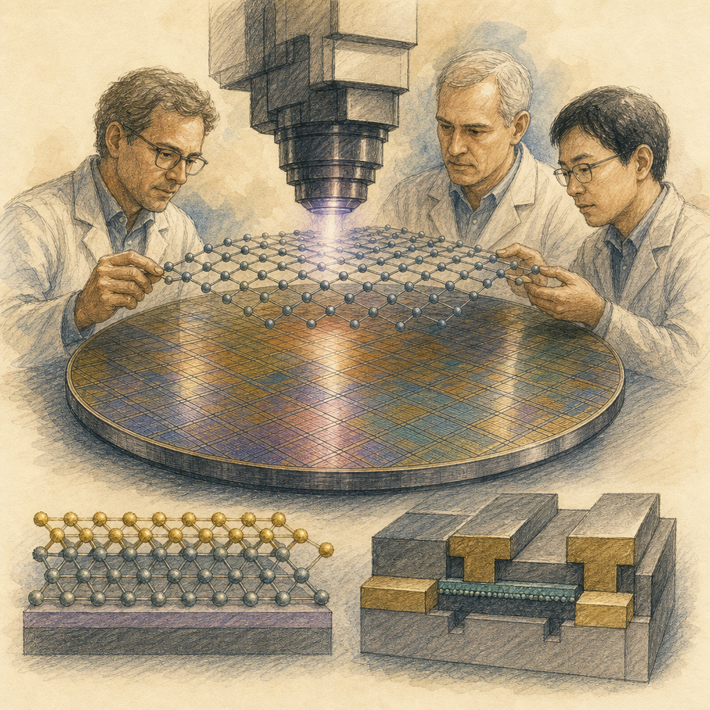
Imec, ASML, and TSMC have reached a milestone in semiconductor development by integrating two-dimensional (2D) material transistors on a single 300-millimeter wafer. The initiative demonstrates the feasibility of manufacturing components with atomically thin channels on an industrial scale, overcoming a major obstacle to the continued miniaturization of chips.
The technology developed by the consortium allows the combination of n-type and p-type transistors using 2D materials on the same silicon base. This complementary integration is a fundamental requirement for building efficient logic circuits, mirroring traditional semiconductor architecture but replacing conventional silicon with alternatives that maintain conductivity even at minimal thicknesses.
The transistors were fabricated with a 50-nanometer pitch (the distance between the centers of adjacent components). Reducing this metric is essential to increase transistor density in a processor, which directly impacts the performance and energy efficiency of future devices.
The industry views the transition to 2D materials as the most likely path to the so-called post-silicon era. As traditional architectures approach their physical limits, 2D channels emerge as a solution to prevent the short-circuiting and current leakage that occur when silicon is scaled down to atomic levels.
Despite this technical breakthrough, the mass production of chips with these characteristics still requires improvements in deposition and lithography processes. However, the collaborative effort between a research institute, the leading lithography equipment manufacturer, and the world's largest foundry indicates that the technology ecosystem is preparing for the transition beyond the current limits of silicon.
What milestone did Imec, ASML, and TSMC achieve with 2D materials?
The consortium successfully integrated n-type and p-type transistors using 2D materials on a single 300-millimeter wafer with a 50-nanometer pitch, proving industrial-scale feasibility.
Why are 2D materials important for the future of semiconductors?
2D materials prevent the short-circuiting and current leakage that occur when silicon is scaled to atomic levels, making them the most likely path for continued chip miniaturization in the post-silicon era.
What is still needed for the mass production of 2D material chips?
Mass production requires further improvements in deposition and lithography processes, despite the successful demonstration of complementary 2D transistors on a 300mm wafer.